Scanning electron microscopy (SEM) is often a first screening inspection for many material issues. Energy dispersive spectroscopy (EDS) is an accompanying elemental analysis technique that detects atomic numbers 6 through 92 with a detectability limit of approximately 0.1 weight percent. The analysis diameter and depth for EDS is typically a few micrometers. Images obtained in backscatter electron mode offer quick identification of areas with different atomic number.
SEM/EDS is an ideal technique for inspections of a wide range of materials. Typical applications include metallic and ceramic failures, electrical contact issues, coatings, polymers and paper products. EDS is a very rapid technique for measuring coating thickness in the range of 1000Å – 20,000Å if standards are available. EDS mapping illustrates the distribution of species in the near-surface region.
For studies that require the best in resolution, field emission scanning electron microscopy is also available. Insulating and fragile samples can be imaged without coating in a variable pressure system.
Scanning Electron Microscopy/Energy Dispersive Spectroscopy Features
- Elemental concentration from atomic numbers 6-92
- 1 -3 µm analysis depth
- Backscattered electron imaging
- Color maps and line scans
Metal Component Failure Analysis
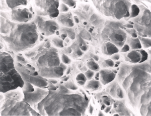
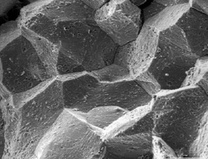
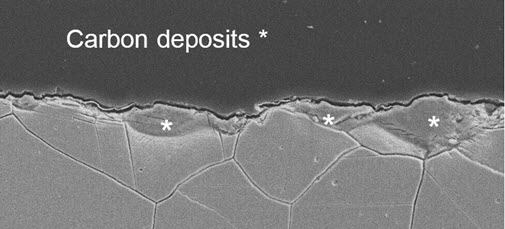
SEM/EDS is one of the primary methods used to inspect failed components in a wide variety of applications. The micrographs below show materials that failed by ductile overload or by grain boundary embrittlement. The cross section illustrates a 330 stainless steel sample exhibiting carbon pick-up in a heat treating furnace.
Paper Coating
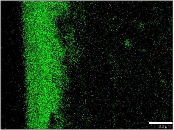
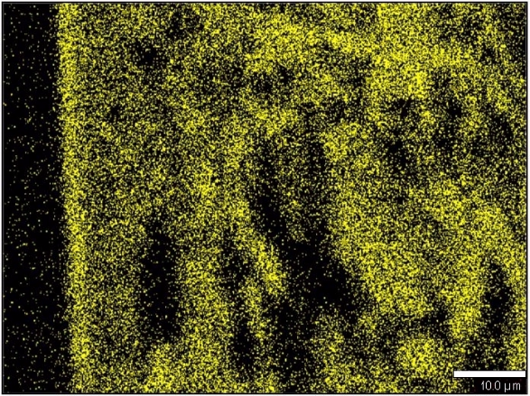
A coated cardboard product was cross-sectioned to investigate the thickness of coating layers (organic top coat, alumino-silicate kaolin, and calcium carbonate subcoatings).
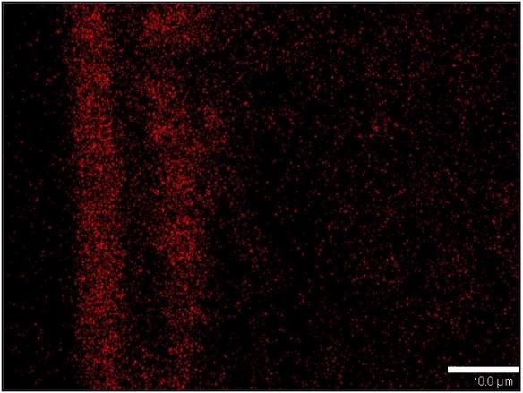
Aluminum map
Calcium map
Silicon map
Carbon map
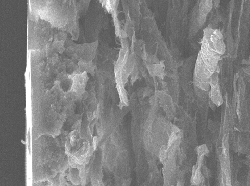
SEM image
